SCN series EMC Scanners are the new industry standard for EMC scanning, with 2D or 4D options.
Pendulum’s DETECTUS EMC-Scanners are high-resolution, affordable scanners that come in three different sizes to fit most DUTs. They combine very-high scan resolution of 0.1 mm with probe head rotation, and the best-in-class scanning software to deliver powerful visualization of the EMC test.
For boards with components of substantially different heights, the optional laser distance meter will enable you to follow the DUT’s topography and measure at a fixed distance from the DUT, automatically creating a precise 3D-model of the DUT. With Pendulum’s DETECTUS EMC-Scanners, you’ll be able to quickly and easily identify any potential problems with your product’s electromagnetic compatibility, ensuring that it meets all applicable standards.
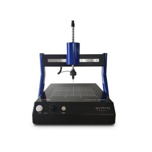
The Pendulum Detectus EMC-Scanners are a complete scanner system that can be used to test the field strength of an object. The system consists of the EMC-Scanner Hardware package, the Detectus Scanning SW (DSS), a Spectrum Analyzer, and a PC to run the scanner SW.
The object to be tested is placed on the coordinate board, and a small near-field probe is moved in a controlled and repeatable path above the test object, registering the field strength. The probe output signal in every position is measured by the Spectrum Analyzer, and transferred to the scanner SW. The smart SW combines the spatial information (X,Y,Z) with the spectrum in that position, and presents detailed results.
Leading Performance from the Detectus designers
With 25 μm step size of the scanner, you can pinpoint emission sources in densely packed designs. You can even follow emission hot spots inside an IC, using the IC option
You can scan emissions up to 10 GHz, with the standard Pendulum Probe kits. If the user has near-field probes going up to higher frequencies, e.g. 70 GHz, these can normally be attached and used for EMC-scanning. The SW has no limits, but you must of course use a Spectrum Analyzer that support the frequency range.
Within the Detectus HRE series you can choose from two different sizes, with or without probe rotation, to fit most test objects. The scan area (WxDxH) is:
- 280x180x85mm (3D or 4D*)
- 390x290x130 mm (3D or 4D*)
* 4D = 3D xyz movement, plus probe rotation 0 to 360o

Advantages of the Detectus HRE scanner
In R&D
Using the EMC-Scanner during the early stages of design enables you to detect potential emission and immunity problems before they become integrated into the product and expensive to correct.
If a product has failed a test at a test house, normally you only learn which frequency failed, not the location of the noise source. The EMC-Scanner can help you find the source, and repeated measurements while redesigning your product helps you lower the emission levels.
Similarly, if your problem was immunity, you can (optionally) scan for sensitive areas and repeat measurements while strengthening your product.
You can compare different design solutions and make comparative measurements of electromagnetic emissions. You can even analyze the EMI-noise inside an IC or a compact module, thanks to the ultra-high-resolution step size (25 μm)
In Q&A
The EMC-Scanner can help you maintain a high quality in the production line. You can make measurements on samples from the production line and easily compare them with a reference. That way you can make sure that, for example, a change of supplier of a component doesn’t affect the emission spectra in a negative way.
World class SW lets you SEE electromagnetic fields
The easy-to-use and feature-rich DSS SW let you measure and visualize the intensity and the location of a radiation source at a component level – or even inside a component. The results of such a measurement can be shown as two- or three-dimensional colored maps. The measurements can easily be repeated creating objective, comparative measurement results.
Measurements can be saved and later compared with board-level changes, thanks to the exact repetitive scanning. The SW even allows to subtract two scanning results to emphasize the true difference of any board layout – or component – change.